|
Shenzhen Wanyuan Electronic Technology Co.,LTD
|
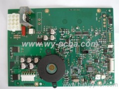
pcba
| Payment Terms: | T/T,L/C,D/P,WU |
| Place of Origin: | Guangdong, China (Mainland) |
|
|
|
| Add to My Favorites | |
| HiSupplier Escrow |
Product Detail
Our PCB got UL,SGS,ISO9001:2000,RoHS and IPC-610 certificates,and are used to a wide range of fields such as computers, digital products,medical equip
PCB process capability:
1.Layer: 2-22 layer
2.Product type: Rigid PCB,High Density Inverter PCB,thick copper PCB
3.Materials: FR-4, CEM-3, Teflon, Aluminum Substrate, Rogers, Halogen Free, High Tg
4.Copper Thickness: 140micron(4oz)
5.Min Board Thickness: 0.4mm
6.Max Board Thickness: 5.0mm
7.Min finished Hole Diameter: 0.1mm
8.Outer layer line width / spacing: 0.1mm/0.1mm
9.Inner layer line width / spacing: 0.1mm/0.1mm
10.Min aperture: 0.2mm
11.Min Laser drilling: 0.1mm
12.Min Ring Width: 0.11mm
13.Min BGA-bit hole spacing: 0.4mm
14.Resistance Tolerance: ±10%
15.Minimum Insulation Thickness: 3mil
16.Maximum laser blind hole thickness to diameter ratio: 0.8:1
17.Maximum working board size: 520*622mm
18.Drilling Tolerance (PTH): ±0.075mm
19.Drilling tolerance (NPTH): ±0.05mm
20.Outline Tolerance (CNC): ±0.13mm
21.Surface coating: Lead Free HAL, HAL, Flash Gold, Immersion Gold, Immersion Tin, Immersion Silver, OSP, Gold Finger Plating, Carbon Ink Printing, Peelable Blue Mask
Didn't find what you're looking for?
Post Buying Lead or contact
HiSupplier Customer Service Center
for help!


